Table Of Content
- Analysis of Switch-Mode Power Supply and Rectification: Transistor Timing & Boost Capacitor Issues
- Design of Analog CMOS Integrated Circuits (Behzad Razavi) (z-lib.org)
- Using PCB Tools for Analog Design
- Analog Design Components
- AN UPDATED COURSE ON ESD FOR ANALOG CIRCUITS NOW AVAILABLE UNDER ACADEMIC COURSES
- Digital-to-digital converter (DAC) circuits
- Why Do Digital and Analog Require Separate Ground Planes?

This tool searches for violations of the design rules, as well as mismatches between the NETLIST and layout. Finally, using the 3D viewer tool, one can verify the final appearance of the PCB, and check if the component spacing is feasible. Cadence PCB solutions is a complete front to back design tool to enable fast and efficient product creation. Cadence enables users accurately shorten design cycles to hand off to manufacturing through modern, IPC-2581 industry standard. This article explains the sources of EMI – specifically radiated emissions – and presents techniques to minimize EMI for an analog signal chain, including detailed layout examples and measurement results. Once you have enrolled in a course, your application will be sent to the department for approval.
Analysis of Switch-Mode Power Supply and Rectification: Transistor Timing & Boost Capacitor Issues
Our TI E2E™ design support forums are an engineer’s go-to source for help throughout every step of the design process. Connect with our engineers or browse through analog-related articles to help you quickly resolve your design issues. This allows the behavior of the circuit to be analyzed using combinatorial and sequential models, only considering two voltages (“one” and “zero”), which substantially simplifies the design and verification process. The primary difference between analog design and digital design is the type of underlying analysis that is used. For five decades, we’ve been honored to be your engineering resource for innovative design.
Design of Analog CMOS Integrated Circuits (Behzad Razavi) (z-lib.org)
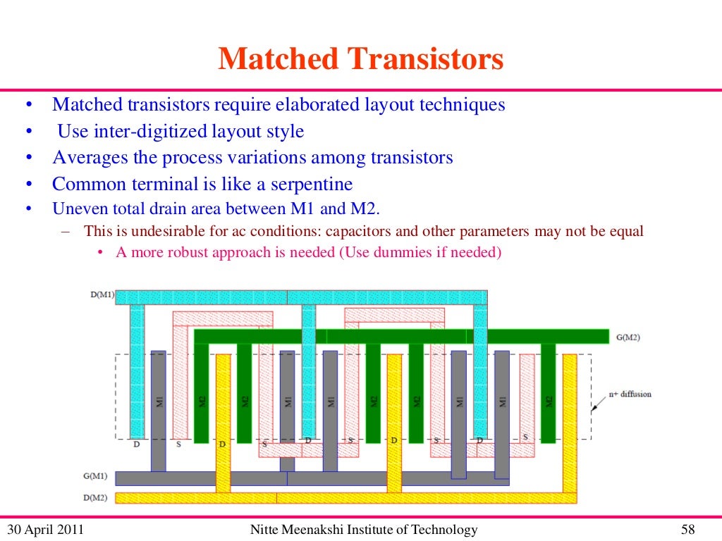
This variability manifests as changes in operating voltage, operating temperature, and in performance. Densely packed devices can also interact with each other and with the silicon substrate, package, and board to cause signal distortions. All of these effects can occur between devices and within a single IC as well. Because analog design requires both intuition and rigor, each concept is first introduced from an intuitive perspective and subsequently treated by careful analysis.
Using PCB Tools for Analog Design
Before enrolling in your first graduate course, you must complete an online application. Please click the button below to receive an email when the course becomes available again. All rights are reserved, including those for text and data mining, AI training, and similar technologies.
Simulation using a SPICE-like simulator is used to verify the clamp models. The second laboratory applies these ESD clamps to design, simulate, and verify the ESD input protection and output protection for an op amp. From the literature we know that second-order active filters can be implemented using the multiple-feedback topology, which requires only one OPAMP and several passive components (Figure 8). Now we need to define the OPAMP model and the value of the passive components. Further, methods exist for correcting this digital degradation that are simply unavailable to analog formats.
This issue features topics from the impacts of ADC noise to comparing dual-supply discrete and integrated instrumentation amplifies. This issue features topics on designing with ADCs along with optimizing battery life in your application. Synopsys is a leading provider of high-quality, silicon-proven semiconductor IP solutions for SoC designs. Both individuals and organizations that work with arXivLabs have embraced and accepted our values of openness, community, excellence, and user data privacy. ArXiv is committed to these values and only works with partners that adhere to them. Filter, compare and select the right product for your design with our selection tool.
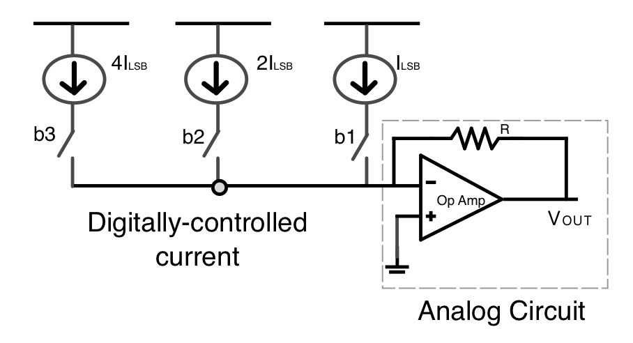
Digital-to-digital converter (DAC) circuits
Cadence Custom/Analog Design Migration Flow Accelerates Adoption of TSMC Advanced Process Technologies - Business Wire
Cadence Custom/Analog Design Migration Flow Accelerates Adoption of TSMC Advanced Process Technologies.
Posted: Mon, 25 Sep 2023 07:00:00 GMT [source]
Take a look back with our first editor and discover some of our favorite articles. Custom Compiler facilitates design/layout collaboration that makes it easy to communicate design intent and achieve analog design closure, as shown below. Our newsletter provides updates on newly available products, solutions, published articles, webcasts and other resources that contribute to innovative design. If you’re an electrical engineering student or recent graduate with an interest in analog electronics, you’re just a click or two away from articles, tutorials, and a wealth of other helpful resources.
From data converters to sensing, beginner to advanced – look to the Analog Design Journal for answers to your analog design questions. Some of the industry’s most knowledgeable engineers share exclusive, carefully curated articles geared toward engineers across all industries and levels of experience. In analog design, circuit stimulus is treated as a continuously varying signal over time.
Analog-to-digital converter (ADC) circuits
Most often, students and hobbyists are likely to begin with analog design due to the straightforward nature of the content of the components. The Synopsys Custom Design Platform is a unified suite of design and verification tools that accelerates the development of robust custom analog designs. This site is dedicated to providing resources for students and professionals in the area of analog integrated circuit design using CMOS and BiCMOS technologies. The resources are designed to help understand the principles, concepts, and techniques of analog integrated circuit design.
The professional resources include online lectures on how to do analog integrated circuit design step-by-step using design procedures. Since all the basic devices in an IC respond to continuous time stimulus, analog design forms the foundation for all IC design. There is significant variability in the manufacturing process for advanced technology nodes. The actual operation of the high number of devices on advanced ICs also causes variability.
It is far from impossible to encounter designs that operate solely in one domain. Mixed-signal technology, as it’s known, incorporates both analog and digital elements into its design, whether this is at the component or board level. Any type of transistor can be applied as an amplifier, a switch, or a voltage-controlled resistor, but some are more fitted to specific applications.
This variation in the gain is acceptable, considering the design specifications of our project. Analog design is one of the most critical blocks in any electronic project. It is the fundamental connection between an idea and the real world. In many cases, even well-conceived schematics and high-quality components fail to achieve their required performance if the analog blocks are poorly designed. Therefore, the objective of this analog design article is to provide a step-by-step guide and useful insights to help you achieve the best performance from your analog circuit design.
The actual devices in any circuit are responding to continuously varying stimulus, so analog circuit design is really the foundation of the design of digital circuits. During the early days of analog circuit design, circuits were developed using hand-made schematics and calculations, without the possibility of simulating before testing. Nowadays, the hardware designer can rely on several digital tools to conduct a project. Schematic CAD (Computer Aided Design) tools can be used to design schematics from scratch.
For the first time in any ESD course a simple snapback model suitable for SPICE or SPECTRE is developed. This model can be independent or dependent on rate of rise of the ESD voltage. Strictly Necessary Cookie should be enabled at all times so that we can save your preferences for cookie settings. While you can only enroll in courses during open enrollment periods, you can complete your online application at any time.


No comments:
Post a Comment